
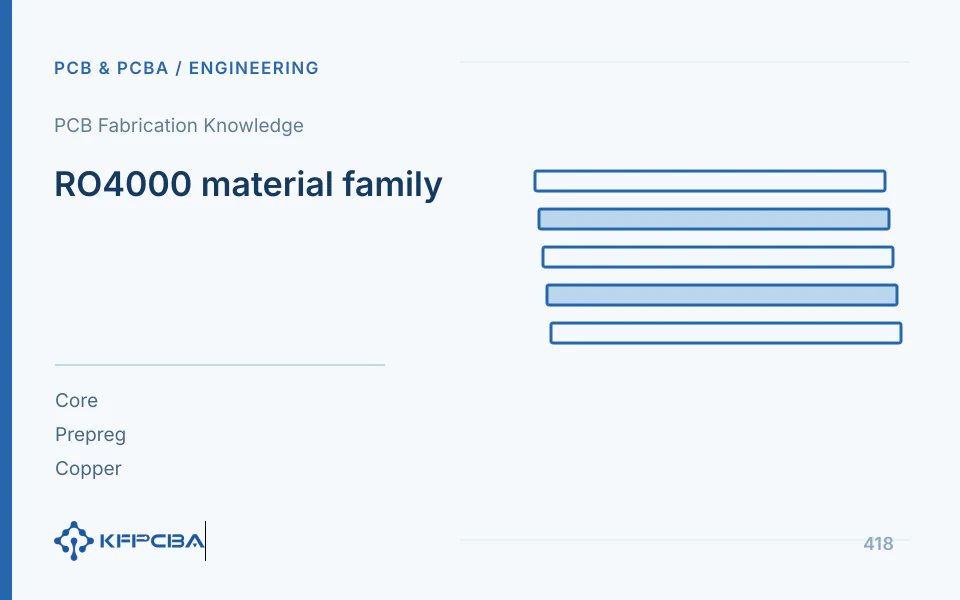
The RO4000 series name identifies a material family; it cannot serve as the complete material specification for a multilayer PCB. Cores support circuitry, bondply bonds adjacent layers, and copper foil forms conductors. Even within the same family, the exact grade, supplied construction, post-lamination dielectric thickness, and fabrication route must be specified before the stackup can be approved.
What problem the core board and bonding sheet each solve
A core already consists of cured dielectric and copper. During lamination, bondply joins adjacent layers and fills the spaces between copper features. Nominal core thickness and the thickness added by bondply after lamination are different measurement quantities. A material table that lists only 'Rogers laminate' omits interlayer bonding requirements and does not provide a one-to-one correspondence between the design model and incoming materials.
| Object | To specify | Verification Focus |
|---|---|---|
| Core board | Full grade designation, dielectric thickness, tolerances, and copper foil on both sides | Dielectric and copper structure and dimensions |
| Bondply | Model number, fiberglass or resin structure, and number of sheets | Fill, post-lamination dielectric thickness, and interface bonding |
| Outer Copper Foil | Category, thickness, surface finish, and lamination system | Adhesion, finished copper, and trace shape |
| Mixed Lamination Materials | Layer-by-layer identity, substitution scope, and thermal process | electrical model and manufacturing compatibility |
The manufacturer's RO4400 bondply literature describes multilayer constructions with RO4000 cores and conditions for combining them with FR-4. This provides a basis for identifying candidate fabrication routes; it does not mean every material combination and ply count has fabrication approval.
Assign materials by signal function rather than distributing them uniformly
First list critical RF layers and their reference planes, then identify low-speed control, power, and mechanical regions. The field distribution of critical microstrip or stripline traces determines which dielectrics actually participate in transmission. If only the surface layer is RF-critical, compare loss, hybrid-lamination risks, and fabrication routes before deciding whether to use the same high-frequency material throughout the board; do not decide on material unit price alone.
Associate each impedance group with its signal layer, reference layer, target impedance, frequency band, finished copper, and transmission-line type. Layer transitions, reference-plane changes, and via structures must also match the model. Changing bondply thickness can change stripline field distribution and impedance even when the core grade remains the same.
Eight-layer structure thickness budget example
For an eight-copper-layer example used solely to illustrate the calculation, assume three cores each with a dielectric thickness of 0.20 mm, four bonding intervals each with a post-lamination dielectric thickness of 0.15 mm, and eight copper layers each 0.035 mm thick. The simple thickness sum is 3×0.20+4×0.15+8×0.035=1.48 mm. This equation checks whether all constituents are included; it does not define a production-ready construction.
To avoid double counting in an actual budget, specify whether core thickness includes copper, whether the outer layers receive additional plating, and whether surface finish and solder mask are included in the measured overall thickness. Also account for individual layer tolerances and the post-lamination thickness distribution. After the fabricator proposes adjustments, the design team should recheck edge connectors, impedance, and assembly, then freeze the revised definition of overall thickness.
Compatibility of mixed lamination is not determined solely by lamination temperature
Differences in resin flow, bonding surfaces, glass weave, and thermal expansion can all affect the result. Sparse copper regions require resin fill, while dense regions can create local thickness differences. Overlapping the recommended temperature ranges for two materials alone does not establish adequate resin fill or interlayer reliability.
- Include full core and bondply designations in the layer diagram, identifying material orientation and each lamination cycle.
- Provide copper artwork or remaining-copper information to review local fill, resin starvation, and thickness variation.
- Confirm the surface treatment, copper foil, and interlayer bonding system, and document the combinations approved by the fabricator.
- Check dielectric thickness, interfaces, hole connections, and impedance at representative locations to establish sample evidence.
The manufacturer's statement of process compatibility is a material-level input. The fabricator must still confirm a process window using its own equipment and the actual combination. In hybrid lamination across suppliers, a shared resin-family name must not be treated as proof of identical construction.
How to freeze a layer-by-layer material list
| Interlayer Position | Mandatory Association | Approval Output |
|---|---|---|
| RF Layer to Reference Plane | Material card, post-lamination dielectric thickness, copper weight, and transmission-line type | impedance calculation and test coupon version |
| Internal Core Board | original part number, structure, and copper foil | Bill of materials and batch records |
| Bonding Interval | Material designation, ply count, copper fill, and lamination route | Target dielectric thickness and cross-section measurement points |
| Full Panel | Total thickness, symmetry, and assembly interfaces | Controlled manufacturing drawings and substitution approval scope |
A procurement substitution requires more than changing the family name at the top of the BOM. Each change must identify the affected layers and material construction, along with the impedance groups and reliability items it affects. Update the documentation package only after the relevant scope is approved, so the design model and shop-floor materials do not become two different revisions.
How to trace back when first article shows discrepancies
If overall board thickness is close to target but impedance is out of specification, the thickness distribution between layers may have changed. Inspect a cross-section of the relevant layers rather than measuring only total thickness at the board edge. For large local impedance differences, check copper distribution and post-lamination fill. For delamination or abnormal hole connections, first investigate interfaces, hole groups, and thermal processing; a material's low Df does not explain mechanical failure.
Separate design inputs, fabrication targets, and measured results in the report, and record material lots and panel locations. Repeat orders can use the approved snapshot, with a difference review when a new material construction is introduced. This preserves consistency with historical orders while preventing database updates from unintentionally changing an existing design.
Stackup reviews must also address nominal units. 1 mil equals 0.0254 mm. When material specifications use inch-based sizes, retain the original nominal value and provide the conversion; do not use a prematurely rounded millimeter value as the center of the manufacturer's tolerance. Software display precision, fabrication drawing precision, and actual allowable deviation are different matters and should be stated separately in the output.
When sharing a stackup in multiple formats, make the PDF, CAD library, and machine-readable file reference the same construction ID, and check that their layer sequences agree. Define top and bottom orientation clearly so different tools do not reverse the layer numbering. After the first import, verify materials and reference planes layer by layer before using automatic impedance solving, which could otherwise produce a formally complete report for a misaligned construction.
If the originally approved material is unavailable for a repeat order, first list candidate constructions and their effects. Do not substitute materials on the production floor based only on similar thickness. Apply the change to subsequent lots only after material, fabrication, and design stakeholders have finalized the same revision.
Give design, procurement, and fabrication different views of the same construction
Designers need dielectric parameters, reference planes, and transmission-line types; procurement needs full grades, supplied constructions, and quantities; fabricators need copper distribution, interlayer bonding details, and process routes. Separate views can make this information easier to use, but all must reference the same stackup ID. Identify the controlled source for each field so the same abbreviation does not represent different items in the three departments.
For example, if a bonding interval uses two plies to achieve the target dielectric thickness, the procurement list should show the actual supplied construction, fabrication records should show the combination and lamination process, and the design model should show the approved post-lamination spacing. The three descriptions need not use identical wording, but they must correspond item by item. If ply count changes, check procurement quantities, the thickness budget, and the effect on the model.
At the end of the review, ask each of the three teams to identify its most sensitive input and verify that it is clearly specified. Design may focus on reference-layer spacing, fabrication on local fill, and procurement on copper foil options. Mark undefined fields for clarification rather than covering them with one series name. This lets future staff understand each material's role from the construction record, even when personnel change.
If a candidate construction has not yet been confirmed by fabrication, label it as planned. Early models remain useful, but must not share the same status as approved orders. Once the final revision is established, retain the differences and reasons between candidate and approved versions for reuse during future material shortages or design upgrades.
Frequently Asked Questions
Is specifying RO4000 plus FR-4 enough?
No. Specify the grade, core and bondply construction, post-lamination thickness, and approved combination for each layer.
Whether the same Dk value can be uniformly adopted for the same series
Data differ by grade and material role and must correspond to the actual layer. For more information, see RO4400 lamination thickness, Manufacturing Combination and Delivery List.
Source material and applicable scope
- Rogers Corporation, RO4000 Series Laminates; version: the current official series webpage does not specify a fixed revision number; checked 2026-10-17; relevant sections: material-family introduction and links to individual grades; scope: supports only family and grade classification. The layer-by-layer list and thickness budget are engineering compilations.
- Rogers Corporation, RO4450F and RO4460G2 Bondply; version: public PDF, with no revision number shown in the cited passage; checked 2026-10-17; relevant sections: page 1 material family, compatibility, and hybrid-lamination guidance; scope: supports core and bondply roles and candidate compatible routes, not approval of arbitrary combinations.
