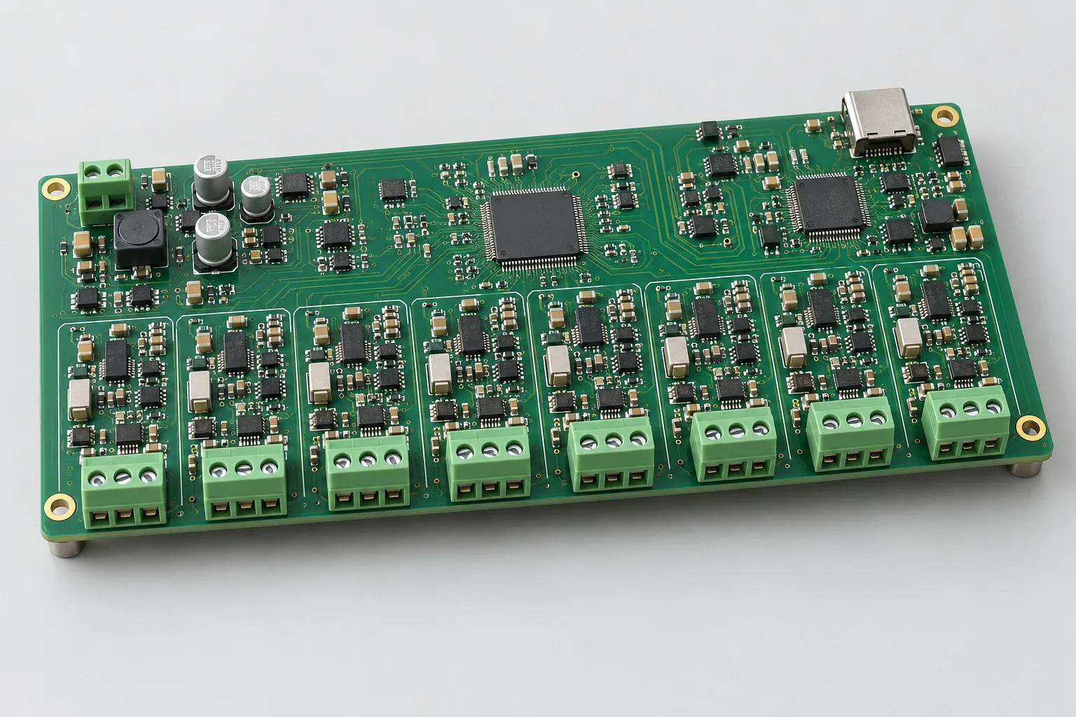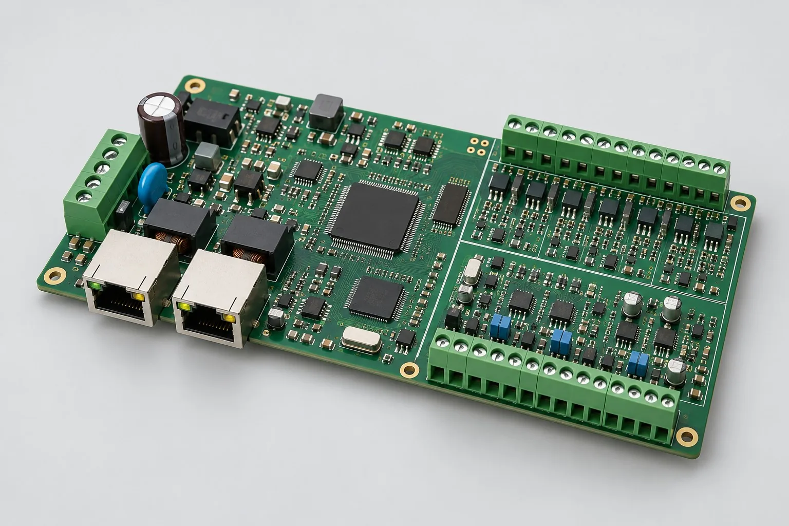
Engineering reference design · prototype validation pending
4–20 mA acquisition board design: four current loops to isolated upload
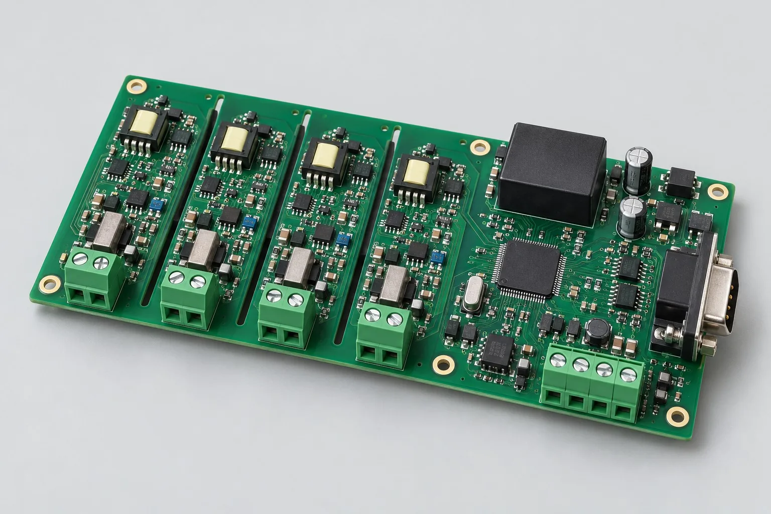
The four-channel 4–20mA acquisition board routes transmitter current through field-side low-side sensing, conditioning, and an ADC to the controller, then uploads through an isolated industrial interface. The basic version shares field ground across all four channels; assess per-channel isolation separately. Output disconnected-sensor states separately from measurements.
Custom development reference design. The following parameters are requirement configurations and design targets; validate functions and performance through agreed prototype tests.
| Functional Partition | Design and Inspection Objects |
|---|---|
| Four-channel current loop terminal | Define two-/three-/four-wire connections, supplies, and compliance voltages for all four transmitters; confirm whether shared field grounding is permitted. |
| Sampling resistor and conditioning | Use Kelvin connections for low-side shunts, with protection and RC filtering; check shunt voltage drops, temperature drift, and input common-mode limits. |
| Field ADC / digitally isolated signals | ADCs sample field-side and transfer through digital isolation; isolation does not replace analog common-mode adaptation. |
| MCU / industrial interface | The controller converts current using calibration coefficients and uploads over isolated RS485; Modbus RTU is an optional protocol. |
| Isolated Power Supply | Separate supplies for the 24V input, field ADC, and isolated communication; use distinct sensor-power and measurement pins to prevent misconnection. |
| Calibration / Disconnected State | Calibrate 4/12/20mA and test opens/overrange; do not treat fault codes as valid zero. Retain coefficients per channel. |
How much does 4–20 mA board design cost, and how is it quoted?
For a 4–20 mA board quotation, first confirm shared field ground or per-channel isolation. The number of isolated supplies and front ends, error targets, protection, and calibration of each channel affect effort; voltage inputs require a different conditioning circuit. List design fees, actual channel calibration, acquisition firmware, and prototype materials separately to avoid comparing prices by channel count alone.
Quotation terms depend on the approved files, quantity, material supply, tests and delivery requirements.
Prepare a structured RFQ or use the short inquiry form.
| Quotation Items | What services are included | What to Check When Comparing Quotes |
|---|---|---|
| Circuit and PCB Design | Current-loop wiring, shared ground/per-channel isolation, and error budget | Reusable portions of existing designs and circuit/mechanical changes |
| Software and Validation | Multi-Point Calibration and Disconnection Diagnosis | Define channel input points, temperature conditions, coefficient retention, disconnection states |
| Prototype Preparation | Bare PCB, BOM procurement, assembly, and agreed prototype quantity | Whether material/component revisions, prototype quantities, and test targets match |
| Subsequent Revision | Record new requirements separately from post-test corrections | How agreed changes, source files, and validation results are delivered |
Should 4–20 mA acquisition share ground or isolate each channel?
Where the field wiring permits a shared ground, compare shared-ground sensing followed by isolated upload. If channel ground-potential conditions prevent this, compare per-channel isolation. The approaches use different numbers of front ends and supplies, so evaluate cost against actual field wiring.
Are 4–20 mA and 0–10 V boards directly interchangeable?
Current inputs use shunt-resistor conditioning; voltage inputs require a separate range and protection review and cannot be supported by rewiring alone. Design dual-mode support as a separate function and calibrate both modes independently.
Does current-acquisition development include calibration?
Specify each channel’s input points, temperature conditions, coefficient storage, and disconnected-sensor states. Encoding resolution is not an error specification; compare quotations using the same multipoint calibration and miswiring-test scope.
Reference: four current loops to isolated upload
| Configuration Field | Reference Configurations/Selections | Basis and Status |
|---|---|---|
| R&D Direction | Industrial process acquisition R&D reference configuration | Illustrative design direction; requirements and prototype validation must be agreed |
| Reference Function | 4 Channel 4–20 mA Transmitter Acquisition | Design Objective |
| Channel Structure | Four shared-ground low-side shunts + digital isolation; assess channel isolation separately | Design Objective |
| Power Target | 24V field input; budget sensor supply separately | Design Objective |
| Sampling-rate target | Per-channel 100SPS target example | Design Objective |
| Frontend Configuration | Precision shunts, RC, clamps, ADC | Design Objective |
| ADC Selection | Multichannel ADC; separate resolution/error budgets | Design Objective |
| Communication Interface | Isolated RS485, optional Modbus RTU | Design Objective |
| Stackup Candidate | 4 Layer, field-side and controller-side isolation barrier defined | Design Objective |
| Diagnostic Function | Underrange/overrange, disconnection, sensor-power faults | Design Objective |
| Calibration Process | Multi-Point Current Calibration and Coefficient Version Records | Design Objective |
| Verify Output | Input error, temperature drift, miswiring, communication tests | Design Objective |
Site Grounding and Per-Channel Isolation
Do not conflate a basic four-channel shared-ground design with per-channel isolation. Compare per-channel isolation costs for sites with significant ground-potential differences.
Evaluate input-shunt voltage drop together with sensor compliance voltage to preserve transmitter operating headroom.
Slow process sampling reduces data volume; define filtering response/fault latency separately.
The basic version places the current-loop shunt near field-side ground, then feeds a low-voltage ADC differential input. Using 50Ω for the reference calculation, 4–20mA produces 0.2–1.0V. Still check differential full scale, pin common-mode limits, and protection conditions for the selected ADC and gain mode. Do not apply the 24V field voltage directly to ADS131M08 inputs. If high-side sensing is required, add a common-mode-compatible amplifier or isolated analog front end and recalculate error and protection. Digital isolation does not replace analog-input common-mode conditioning.
Design budget and trade-off examples
Check design targets with engineering calculations
With an assumed 100Ω shunt, 4–20 mA becomes 0.4—2.0V; full-scale dissipation is 0.02²×100=0.04W.
Conditions and Scope of Application:100Ω is an independent power/range example and must not be mixed with the earlier 50Ω input example. Also check loop voltage headroom, protection voltage drops, resistor accuracy/temperature drift, and ADC range; disconnected and overrange states must remain distinct from normal zero readings.
Replace examples with selected components and record margins; calculations support design choices, while prototype records support acceptance.
Power/layout for four loops to isolated upload
- Place protection components near terminals; use Kelvin shunt connections and route return paths to avoid channel crosstalk.
- Keep isolated-supply noise away from the ADC reference; maintain copper keepouts on every layer across the isolation barrier.
- Clearly separate external sensor-power and measurement-input pins to prevent miswiring 24V into the ADC.
Current loop acquisition board R&D input
- Two-/three-/four-wire transmitters, power, and compliance voltage
- Field ground differences, isolation, protection tests
- Measurement error targets, update rate, and temperature range
If circuit files exist, provide editable schematics, PCB, BOM, and current issues, and agree on review or revision scope. If only functions are defined, freeze this page's inputs before selection and circuit development. Agree separately on control-software and external-application responsibilities, interfaces, and acceptance.
Current loop acquisition board phase delivery
| phase | Engineering Work for This Proposal | Reviewable Deliverables |
|---|---|---|
| Requirements and Design Freeze | Freeze wiring, measurement range/error, field ground-potential differences, isolation approach, and update rate | Functional/interface requirements, mechanical revision, acceptance conditions, and open items |
| Schematic and Component Selection | Design low-side shunts/protection/ADC, digital isolation, RS485, power domains | Editable schematics, controlled BOM, footprint checks, and design calculations for these circuits |
| Layout and Routing | Implement four-channel Kelvin sensing, protection return paths, and isolation on every layer; clearly label power/measurement pinouts | PCB source files, actual stackup/hole/net constraints, DRC, and assembly-dimension checks |
| Simulation/Calculation | Budget loop headroom, ADC common-mode/range limits, temperature drift, and communication tasks | Design calculations/models, input conditions, margins, and items awaiting measurement |
| Prototype and Software | Build a four-channel acquisition prototype and integrate conversion, calibration storage, open-wire diagnosis, and industrial upload | Manufacturing package, four-channel acquisition prototype, agreed acquisition/diagnostic firmware, wiring/register tables, per-channel calibration coefficients, and recovery instructions |
| Testing and Version Closure | Calibrate each channel and measure temperature drift; verify miswiring recovery, power-loss recovery, and data integrity under approved common-mode conditions | Procedures, wiring, raw results, and decisions for the prototype revision; include issue/change and limitation lists |
Current loop calibration and disconnection verification
- 4/12/20mA multipoint and out-of-range measurements
- Temperature-dependent error, zero/gain calibration
- Open/short/miswired ports and sensor power loss
- Isolated communication, common mode, power interference
Calibrate each channel and measure temperature drift; verify miswiring recovery, power-loss recovery, and data integrity under approved common-mode conditions. Document equipment, conditions, revisions, and acceptance criteria in the report, including passed items and untested conditions.
Current Loop Calibration and Open Wire Verification Worksheet
The table below breaks four-channel current-loop acquisition and isolated upload into actionable checks. Freeze samples, equipment, environment, and allowable deviations before testing; link results to this revision’s raw records.
| Verification Object | Pre-Production Freeze | How to Test Prototypes in Practice | Delivery and Acceptance Records |
|---|---|---|---|
| Range and Powering | Four-channel shared/per-channel isolation, 2/3/4-wire transmitters, input errors | Apply 4/12/20mA to each channel; test defined out-of-range and temperature points | Deliver channel calibration and supply wiring diagrams; record shared-ground and per-channel-isolated versions separately |
| Disconnection and Miswiring | Open-wire thresholds, protection, sensor supply limits | Simulate open ports, sensor power loss, and approved miswiring | Retain status codes, sampled values, and recovery records; distinguish fault readings from normal data |
| Common Mode and Communication | Ground differences, isolation approaches, RS485 conditions | Run approved common-mode interference plans during continuous upload | Deliver communication errors, sampling offsets, and test setups; an isolator IC alone does not establish board-level isolation |
Manufacturing and assembly coordination for this design
- Identify shunt accuracy/temperature drift and reference-component lots; resistance alone is insufficient for approving substitutions.
- Use a traceable current source in the fixture; retain separate calibration coefficients and test records for all four channels.
Link design revisions to schematics, BOM, PCB, fabrication, and software documentation. When fabricators adjust stackup, materials, or holes, or Assembly parties propose substitutions, recheck critical electrical and test conditions together.
Common questions on purchasing and customization
How much does 4–20 mA board design cost, and how is it quoted?
A project-specific quotation requires review of the available files, quantity, materials, requested tests, delivery destination, taxes, shipping, and trade terms. Complete development separately prices circuits, firmware, prototypes, and verification. Any formula on this page organizes cost inputs; it is not a quoted rate.View cost items, calculation conditions, and sources.
Should 4–20 mA acquisition share ground or isolate each channel?
Where the field wiring permits a shared ground, compare shared-ground sensing followed by isolated upload. If channel ground-potential conditions prevent this, compare per-channel isolation. The approaches use different numbers of front ends and supplies, so evaluate cost against actual field wiring.
Are 4–20 mA and 0–10 V boards directly interchangeable?
Current inputs use shunt-resistor conditioning; voltage inputs require a separate range and protection review and cannot be supported by rewiring alone. Design dual-mode support as a separate function and calibrate both modes independently.
Does current-acquisition development include calibration?
Specify each channel’s input points, temperature conditions, coefficient storage, and disconnected-sensor states. Encoding resolution is not an error specification; compare quotations using the same multipoint calibration and miswiring-test scope.
How should transmitter wiring be checked on a current-acquisition board?
Define two/three/four-wire supply/measurement terminals and normal/disconnection/miswiring plans per channel; prevent 24V reaching ADCs.
Which regression tests are needed after changing a 4–20 mA acquisition board’s shunt?
Resistance, accuracy, and temperature drift all affect measurement range and error. After replacement, recheck ADC input range and loop headroom, and update calibration.
What supporting work can be reduced if the customer supplies a calibration source for four current loops?
Provide the current source’s measurement range, accuracy basis, wiring, and valid status; confirm whether 4/12/20mA and out-of-range stimuli cover this design. This may reduce source procurement or some preparation work, but four-channel coefficient calculation, writing, temperature records, and disconnected-sensor records still require execution. Confirm shared-ground and per-channel-isolated wiring separately; delivery of the source does not mean calibration is complete.
What constraints must customers provide for current-loop layout only?
Provide the shunt resistor, ADC range/common-mode limits, transmitter compliance voltage, protection, and isolated power design; freeze the 24V sensor terminals and measurement pinout. Layout implements four-channel Kelvin connections and copper keepouts. Digital isolation does not replace analog common-mode adaptation, and 24V must not connect directly to the ADC.
What acquisition firmware is still needed if Modbus software already exists?
Each channel still needs 4/12/20mA coefficients, unit conversion, disconnected/overrange codes, and coefficient version storage. The communication stack may be reusable, but field wiring and states during sensor power loss require integration. Do not return a fault as normal zero or substitute encoding resolution for calibration.
Which calibration records should accompany 4–20 mA board source files?
Retain shunt accuracy/temperature drift, ADC gain and common-mode limits, isolation approach, and terminal connections. Include channel coefficients and diagnostic mappings with the firmware. Link each channel’s report to its current source, temperature points, input values, and errors. Label the 50Ω and 100Ω calculation examples separately; they are not one actual configuration.
How should added 0–10 V compatibility be requoted?
Add voltage division or conditioning, protection, and input selection; recheck ADC range and miswiring, then establish voltage calibration and state rules. Existing current-loop communication tools may be reused, but front ends and mode-specific tests require separate development. Rewiring or changing conversion formulas alone does not provide reliable dual-mode operation.
Can a four-channel shared-ground board be reused directly where field ground potentials differ?
First confirm common-mode conditions and permitted grounding; if unsuitable, compare per-channel isolation or independent front ends. Parts of the low-side ADC, digital isolation, and RS485 upload may be reusable, but channel-to-channel isolation requires redesigned supplies and measurement chains. Isolated communication does not make the basic shared-ground version individually isolated.
How should I prepare an RFQ for 4–20 mA design?
Start with the target functions, application, and available files. An engineering quotation then confirms two-/three-/four-wire transmitter types, supplies, and compliance voltages; field ground-potential differences, isolation requirements, and protection testing; and measurement error targets, update rate, and temperature range. For an existing circuit, provide editable schematics, PCB files, and BOM. For a faulty prototype, include its revision and reproduction records. List missing information as review tasks so both parties quote against the same assumptions.
How should 4–20 mA acquisition board prototype verification costs be compared by operating condition?
Fix the prototype quantity, revision, equipment, and source of acceptance criteria before comparing costs. Check at least these areas separately: range and power—freeze four-channel shared-ground/per-channel isolation, 2/3/4-wire transmitters, and input errors, then apply 4/12/20mA to each channel and test defined out-of-range and temperature points; disconnection and miswiring—freeze disconnection thresholds, input protection, and sensor supply limits, then simulate open ports, sensor power loss, and approved miswiring; common mode and communication—freeze field ground-potential differences, isolation approach, and RS485 conditions, then execute the approved common-mode interference plan while continuously uploading. State whether raw data and issue closure are included; one successful power-on does not constitute complete verification.
Compare related designs and plan the next step
Eight-channel simultaneous monitoring and acquisition board design · Industrial Ethernet main controller board design solution
Return to multi-layer PCB design selection · Select solution by device function · Consult This Proposal R&D Team
Engineering reference | ADS131M08 component reference: selection conditions and board-level verification: ADS131M08 references ADC/filter/interface only; never apply 24V directly. High-side inputs need extra common-mode conditioning/analog isolation.