Engineering Selection Reference
Ten-layer segmented gold finger PCB: engineering review
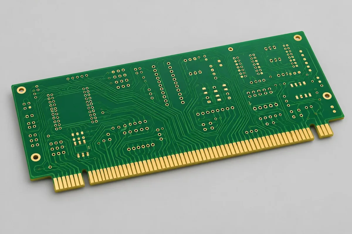
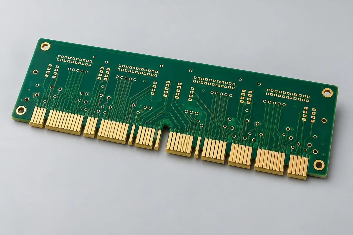
Define separated contact regions, finger lengths and actual connector mating sequence independently. This illustrative ten-layer configuration does not establish KFPCBA production history, hot-swap function or mating life.
All numeric and material callouts below are illustrative, unverified review inputs. They are not evidence of KFPCBA delivery, measured performance, certification or current manufacturing limits. A new order requires approved drawings and confirmation of the complete process combination.
Illustrative configuration inputs
| Review item | Illustrative input and unresolved conditions |
|---|---|
| Illustrative layer count | 10 layers |
| Candidate laminate | TU-872; exact grade unverified |
| Reference feature | Segmented gold-finger contacts |
| Candidate surface zoning | ENIG soldering regions and separately specified finger gold; thickness and hardness unverified |
Review the engineering boundaries
Segmentation, long/short fingers and sequenced contact are different definitions. Verify board-edge datums, insertion direction, slot contact positions, bevels, segment gaps and surrounding clearances from drawings. ENIG thickness in a soldering region does not establish contact wear resistance.
Required RFQ inputs
Provide mating-slot drawing, insertion direction, contact functions and sequence, segment dimensions, finger lengths, board thickness/tolerance, bevels, finish zones and nickel/gold thickness and hardness requirements.
Acceptance and traceability
Agree on dimensional and coating measurements, representative mechanical fit, actual contact behavior and required electrical checks. System-level sequence or hot-swap validation remains separate from bare-board fabrication.
Engineering review scenario
If a revised slot contacts a short finger too early, compare slot contacts, board-edge datum and insertion motion before shortening the finger. Check effective contact length and system states together.
This scenario explains a review method; it is not a documented defect or test result from a KFPCBA project.
Quotation and delivery scope
Itemize materials, fabrication, engineering preparation, agreed inspections, reports, packaging, taxes and freight. Identify quantity units, drawing revision, approved deviations and tooling ownership. Assembly, software and complete-system validation are separate unless expressly included. No published unit price, schedule or capability guarantee is established by this reference.
Contact and soldering surface zones · Gold-finger quotation scope
Submit fabrication files for review or use the short project inquiry. Identify this reference page and list the inputs still to be defined.