Engineering Selection Reference
M.2 gold-finger PCBs: fabrication review for six-layer M.2 gold-finger boards
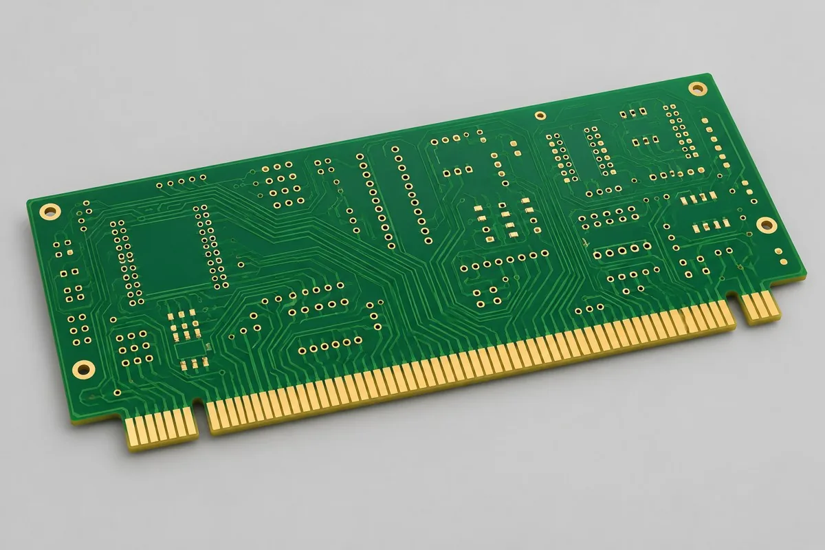
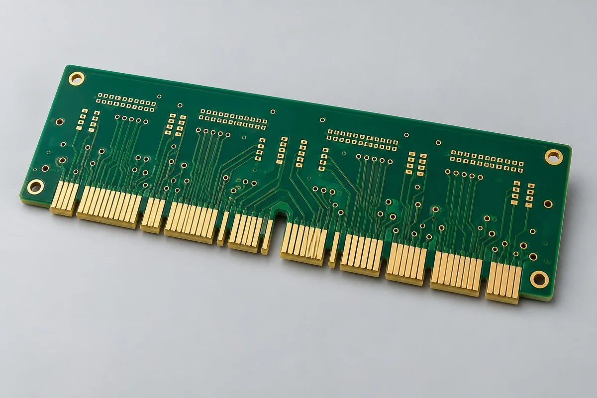
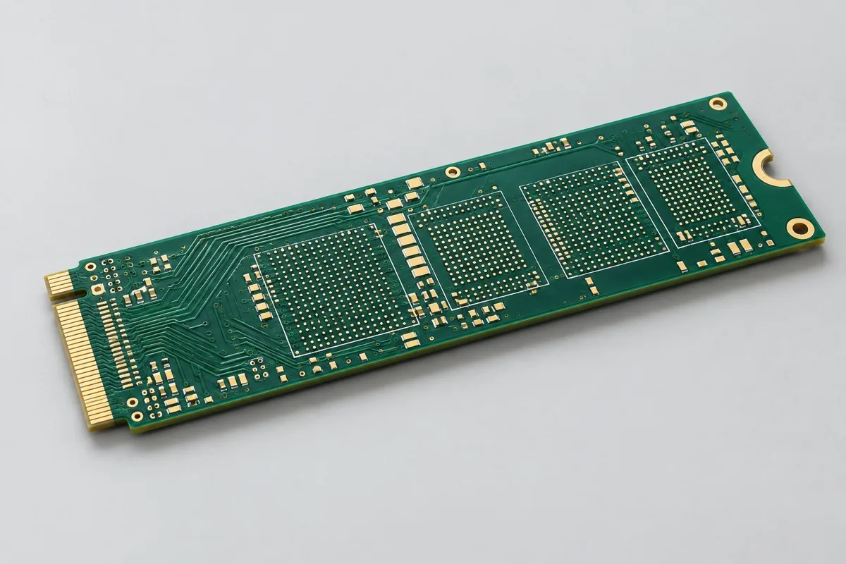
Review six-layer M.2 gold-finger PCB fabrication against the current fabrication drawings. Six-layer M.2 storage bare PCBs require the mechanical revision, mating slot, and PCIe specifications, with separate acceptance of keying, hard gold, and links. The 0.80mm and 85Ω values are reference starting points. Review thin-board support and loss together. Deliver board-edge dimensions, plating, and TDR results; validate SSD functions separately in the system.
First define bare PCB prototyping or production scope for M.2 gold-finger PCBs. Provide Gerber data, drill files, board outline, and layer stackup, materials/processes, quantity, and fabrication acceptance requirements. Thin six-layer storage cards balance slot/contact and link loss; industrial card thickness cannot be reused
Begin six-layer M.2 review with 0.80mm and PCIe 85Ω references. Complete RFQ files with M.2 mechanical revisions and storage specifications. Following specification/input tables link design targets to inspections.
Why choose this structure for M.2 storage cards?
M.2 thickness, keying, and high-speed contacts are closely linked. Evaluate six-layer 0.80mm low-loss gold-finger boards, locking interface revisions and PCIe reference impedance, with procurement focused on thin-card fit and high-speed links rather than shrinking industrial cards.
What does M.2 gold-finger PCB fabrication pricing include?
Costs include six-layer low-loss materials, thin-board control, key/finger profiling, selective hard gold, other-pad ENIG, and specified PCIe coupons. Controllers, flash, firmware, and host verification are separate assembly/development work. Bare PCB prices cannot answer SSD retail prices. Specify mechanical revisions, length, quantity, and plating areas.
Quotation terms depend on the approved files, quantity, material supply, tests and delivery requirements.
Prepare a structured RFQ or use the short inquiry form.
Enter the following items in one itemized quotation: specify cost units and tax/shipping basis, with separate columns for first orders and same-revision repeat orders. The table is a procurement breakdown method, not a ready-made price list; reference specifications require approval against current fabrication drawings.
| Quotation items and scope | Inputs to confirm for this configuration | Same-revision reorders and changes |
|---|---|---|
| Materials/fabrication, quoted per batch or accepted board | Isola I-Tera MT40 low-loss FR4 reference candidate; 6 layers; inner copper 18µm; outer base 18µm/finished target 35µm | Recurs on repeat orders; material, layer-order, or copper-weight changes require requotation |
| Holes and forming, per approved hole table | Ø0.20mm through-holes; minimize PCIe signal layer transitions | Repeat orders use the same fabrication revision; review processes before M.2 mechanical changes |
| Surface finish/packaging, noting areas and batches | Finger hard gold Ni3–6µm/Au0.76µm reference target; ENIG elsewhere | Incurred by actual batch; confirm packaging, storage conditions, and surface-finish substitutions separately |
| Engineering/tooling preparation, identifying one-time or per-batch charges | M.2 mechanical revision: provide keying, edge length, mounting holes, and mating connector drawings to define 0.80mm tolerances. | Verify file revisions, ownership, and storage condition before reusing old tooling; do not assume reuse is free |
| Structural/special inspections, identifying coupons, hole groups, or samples | Record keying, relative finger positions, and thickness after profiling. List impedance/coupons separately from hard-gold thickness/measurement methods. | List initial prototype validation and per-batch sampling separately; quote per-board requirements separately rather than assuming everything is completed once |
| Delivery scope, reports, and accepted quantity | Six-layer storage bare PCBs, key/finger drawings, low-loss material records, plating/TDR data; optional interface test structures. | Retain revision links and batch records on repeat orders; list component assembly, firmware, and complete-unit testing separately |
How do thin M.2 and industrial card PCBs differ?
M.2 has specific keying/thin-board constraints; industrial cards reference 1.60mm/chassis slots. Shrinking outlines does not make them interchangeable. Accept links/plating separately; low loss does not replace proper slots. Define structures by actual controller/connector revisions.
| Comparison Dimension | M.2 Gold Finger PCB Fabrication | Industrial gold finger PCB fabrication |
|---|---|---|
| Material and Grade | Isola I-Tera MT40 low-loss FR4 reference candidate | Isola 370HR FR4 |
| Layer Count and Structure | 6 Layer | 8 Layer |
| Hole Structure and Dimensions | Ø0.20mm through-holes; minimize PCIe signal layer transitions | Ø0.30mm through-holes; no holes/solder mask in finger areas |
| Application | M.2 storage interfaces; embedded SSD bare boards | Industrial I/O expansion cards; chassis backplane cards |
How should M.2 thickness and PCIe impedance be selected?
Mechanical drawings set thickness/keying; controllers/interfaces set impedance. The 0.80mm/85Ω values are references. Determine geometry from signal-ground dielectric/copper thickness. Low loss/fewer transitions serve budgets. Do not change thickness to 1.60mm while keeping outlines or guarantee 85Ω for all revisions.
| Review step | Project inputs | Reviewable output |
|---|---|---|
| 1 Define use and scope | Provide keying, edge length, mounting holes, and mating connector drawings to define 0.80mm tolerances. | Record keying, relative finger positions, and thickness after profiling. |
| 2 Confirm structural requirements | Separate high-speed and contact-plating acceptance; identify contact solder-mask keepouts. | List impedance/coupons separately from hard-gold thickness/measurement methods. |
| 3 Match signal nets to fabrication targets | PCIe 85Ω differential selection target, finalized in writing by controller/interface revision; TDR + link verification | Provide target nets, layer pairs, and verification scope; review with Ø0.20mm through-holes and fewer PCIe transitions |
| 4 Confirm quotation and approved revision | Isola I-Tera MT40 low-loss FR4 reference; 0.80mm target, verify connector mechanical revision; Ni3–6µm/Au0.76µm hard-gold reference; ENIG elsewhere | Request quotations using material/pattern/inspection lists at the same revision; list unapproved substitutions as separate alternatives rather than including them in the baseline quotation |
M.2 storage card manufacturing specifications
| Specification | Reference configuration or target |
|---|---|
| Material and Grade | Isola I-Tera MT40 low-loss FR4 reference candidate |
| Layer Count and Structure | 6 Layer |
| Total Board Thickness | 0.80mm reference target; verify connector mechanical revision |
| Dielectric thickness and interlayer relationship | High-speed signal-to-ground target 0.10mm; symmetric stackup |
| Base Copper and Finished Copper | Inner copper 18µm; outer base copper 18µm/finished target 35µm |
| Hole Structure and Dimensions | Ø0.20mm through-holes; minimize PCIe signal layer transitions |
| Trace Width and Spacing | 0.10/0.10mm reference design |
| Impedance target and measurement method | PCIe 85Ω differential selection target, finalized in writing by controller/interface revision; TDR + link verification |
| Surface Finish | Finger hard gold Ni3–6µm/Au0.76µm reference target; ENIG elsewhere |
| Application | M.2 storage interfaces; embedded SSD bare boards |
| Deliverables | Six-layer storage bare PCBs, key/finger drawings, low-loss material records, plating/TDR data; optional interface test structures. |
Tradeoffs between thin-board support and connector link loss
85Ω is a reference finalized by controller/interface documents. Thin boards increase warpage/support sensitivity. Low loss cannot compensate connector/via losses; hard-gold thickness is not interface certification.
Edge keying, bevels, and foil revisions: fabrication inspection
Match fingers/thickness/bevels to connector drawings first. Minimize differential transitions; models define pads/returns. Freeze low-loss grades/foil revisions rather than retaining only the FR4 category.
Contact plating, keying, and differential TDR: acceptance items
Measure contact thickness/plating/keying; apply differential TDR/S-parameters to specified links. Speed/error tests run on complete SSDs/hosts. Bare board reports cover agreed fabrication/electrical structures only.
M.2 storage card delivery scope
Applications: M.2 storage interfaces; embedded SSD bare boards.
Six-layer storage bare PCBs, key/finger drawings, low-loss material records, plating/TDR data; optional interface test structures.
M.2 mechanical revisions and storage specifications: RFQ inputs
Submit M.2 mechanical revisions/storage specifications to turn targets into inspectable drawings. Inputs below define pattern/material/structural inspections. Freeze quote revisions with approved drawings.
| Required project inputs | Engineering Decisions Affected | Records/delivery as agreed in the order |
|---|---|---|
| M.2 mechanical revision | Provide keying, edge length, mounting holes, and mating connector drawings to define 0.80mm tolerances. | Record keying, relative finger positions, and thickness after profiling. |
| Storage link and hard gold | Separate high-speed and contact-plating acceptance; identify contact solder-mask keepouts. | List impedance/coupons separately from hard-gold thickness/measurement methods. |
M.2 gold-finger fabrication: pricing, selection, and purchasing FAQ
What does M.2 gold-finger PCB fabrication pricing include?
A project-specific quotation requires review of the available files, quantity, materials, requested tests, delivery destination, taxes, shipping, and trade terms. This is not a complete finished-product quotation. Base fabrication/sample pricing, special processes, and inspections must not be billed twice. Any formula on this page organizes cost inputs; it is not a quoted rate.View cost items, calculation conditions, and sources.
How do thin M.2 and industrial card PCBs differ?
M.2 requires thin boards, keying, and specific interfaces. Industrial slots/1.60mm references differ; shrinking does not suffice. Loss/plating do not replace fit. Define links/edges with actual controllers/connectors. View Specific Comparison Basis
How should M.2 thickness and PCIe impedance be selected?
Slot drawings define thickness/keying; controllers/interfaces define impedance. Check separately. The 0.80mm/85Ω values are references. Recalculate geometry after ground-spacing changes; do not promise all M.2 versions equally. View Specific Comparison Basis
Can M.2 PCB quotes include working SSDs?
Discuss PCBs, parts, BGA assembly, firmware, and system verification separately. This bare board reference is not an existing finished SSD. Define controller/flash BOMs and scope before total prices.
Does M.2 gold thickness establish PCIe speed?
Plating serves contacts. Speed also depends on controllers, materials, connectors, and vias. Separate plating measurements from TDR/S-parameters/host errors.
How can M.2 boards avoid failing slot fit after soldering?
Check thickness, keying, mounting holes, and fingers to mechanical revisions, with thin-board supports. Recheck warpage/actual slots after assembly; bare outline acceptance is insufficient.
Should M.2 procurement lock mechanics or 85Ω first?
Check keys, edges, holes, and thickness with mating slots, then controller/PCIe impedance and link budgets. Approve both. The 85Ω reference cannot fix mechanical incompatibility; gold thickness does not prove speed.
How do per-board and per-panel M.2 fabrication quotes convert?
Review keys, holes, effective finger lengths, and plating leads with panels; list support/coupons separately. Quotes state finished boards per panel, purchased panels, and board/panel delivery. Divide actual panel fabrication by accepted boards for unit cost. List setup/special inspection/packaging separately; theoretical utilization does not guarantee yield.
How should M.2 first-order setup and repeat costs be separated?
Confirm M.2 mechanics, links, and hard-gold files first, identifying one-time engineering/tool/test charges. Record profiled keys/fingers/thickness. Verify approved files/ownership before reuse. Current materials, fabrication, and inspections still incur costs. List new setup separately; old totals alone are insufficient.
Can I get M.2 fabrication budgets before M.2 mechanical files are complete?
Describe use, outline, quantity, and drawings for a budget listing gaps. Formal review needs keys, lengths, holes, and connectors to set 0.80mm tolerances. Deliver profiled key/finger/thickness records. Confirm fabrication/inspection after freezing conditions. Initial inquiries need not have all files, but estimates exclude undefined structures.
What needs reconfirmation after material, drill, or mounting changes on repeat M.2 orders?
Separate link/plating acceptance and mask keepouts. List impedance/coupons and gold thickness/methods separately. Map changes to old material/drill/mechanical files, identifying drawing/process/measurement changes. Product names/layers alone do not establish equal repeat conditions.
What else needs checking if two M.2 quotes use equal materials?
Compare M.2 mechanics/slot tolerances, then controller PCIe targets/materials/gold. The 0.80mm/85Ω values are references. Bare board prices exclude working SSDs.
Which reports need board IDs before M.2 production?
Record profiled keys/fingers/thickness; separately list impedance/coupons/gold/methods. Link lots, drawings, and results to current IDs. Production uses closed-issue revisions. Old coupon/artwork reports aid comparison, not current inputs. Define uncovered product scope separately.
Do lower low-volume M.2 prices actually reduce total purchasing cost?
Separate M.2 bare boards, controller/flash assembly, firmware, and hosts. Lower PCB prices need not lower complete SSD costs equally. Sum setup/fabrication/agreed tests/packaging/shipping, divide by accepted quantity, and compare same-scope totals/unit allocations. Use current RFQ rates, without fixed reductions.
M.2 storage cards compared with related board types
Current difference: thin six-layer cards balance slots/contacts/loss; industrial thickness is unsuitable
- Eight-Layer Industrial I/O Hard Gold Insert Card Board — Thickness/bevel/hard-gold contact regions address repeated mating; soldering regions use ENIG separately
- Four-Layer Tiered Gold Finger Test Adapter Board — Long/short fingers establish contact sequencing; frequent test-adapter mating needs separate wear tests
Gold Finger PCB Complete Product Catalog · All PCB Products
M.2 storage card materials and design basis
- Engineering reference | General high-speed interface layout: return paths, length, and layer transitions: Design methodology
- Engineering reference | Basic PCB design rules: copper weight, spacing, and hole diameter: General manufacturing design method
- Engineering reference | I-Tera MT40 fabrication: dimensional compensation, lamination, and drilling: grade reference; unverified material values are not cited
Record material revisions/conditions for six-layer 0.80mm/PCIe 85Ω references. First articles focus on contacts/keying/TDR. Update drawings/tests before release after material/copper/hole changes.
Request Quote for This PCB Configuration: reference product ID 345, include critical circuits/interfaces and quantities, and list retained/adjusted specifications.