
SLLA414A supports reviews of high-speed channels containing signal conditioners and USB hubs. Review the complete path from transmitter package to receiver package, including connectors, protection, coupling capacitors, vias, and cables. USB, HDMI, DisplayPort, PCIe, and SATA cannot share one set of length and impedance values; define protocol and target rate first.
Draw the end-to-end channel before checking local routing
List transmitters, PCB segments, connectors, cables, protection, multiplexers, redrivers, and receivers in signal order. Draw every reversible or switchable path state separately. Loss/distortion budgets differ before and after a conditioner; simply adding two PCB segments does not establish that the device can compensate.
Inputs include actual stackup, dielectric and copper weight, connector models, channel models, device datasheets, and data rate. Outputs should identify each segment's length, reference layer, loss, discontinuities, and remaining budget. This identifies which segment needs changes, beyond merely requiring differential length matching. Bind conditioner equalization, output amplitude, and firmware configuration to board revisions too.
Review reference continuity and return paths at layer transitions together
| Channel Location | Verification Issue | Output Record |
|---|---|---|
| Same-Layer Straight Segments | Whether continuous ground exists beneath the route, without splits or voids | Reference layer screenshots and exception locations |
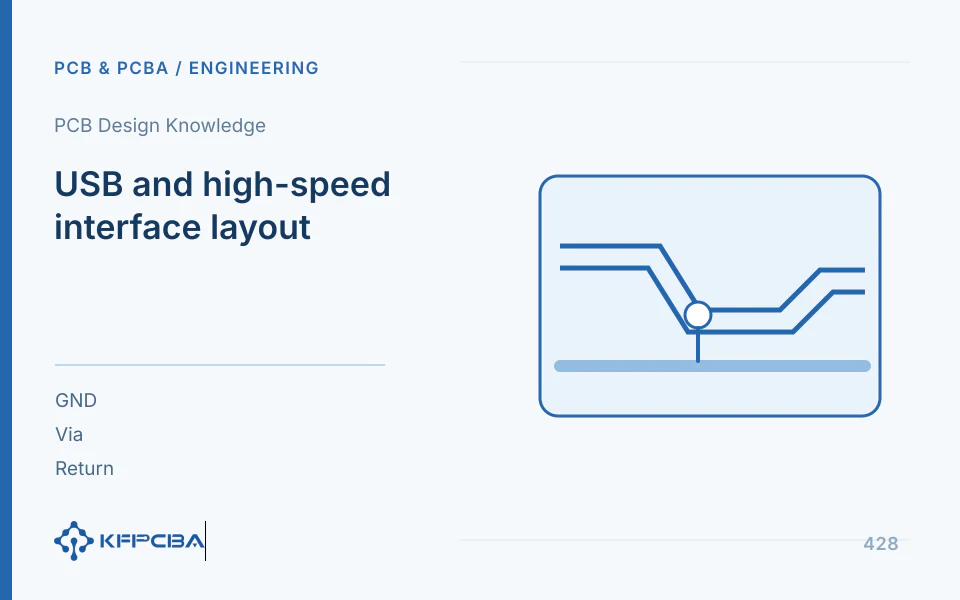
| Signal Via | How reference planes connect before and after layer changes | Ground return via location, quantity, and spacing |
| Connector Exit | Whether ground is continuous beneath pads and the breakout creates long stubs | Connector cross-section and exit layer |
| Component Pad | Whether wide pads and trace transitions are abrupt | Dimensions, anti-pad, and modeling basis |
The guide favors continuous GND reference throughout high-speed routes. When switching between ground planes, place ground-return vias symmetrically beside signal vias. Within 200 mil is the guide's starting point, not a universal optimum. This equals 5.08 mm, but actual designs generally need closer placement according to via geometry, fabrication spacing, and impedance.
If the reference plane is split, adjust the route or plane first. Differential traces do not cancel every return-path problem; common mode, electric-field coupling, and imbalance remain. Reassess returns when power references change; ground-plane stitching methods cannot be copied directly between planes at different potentials.
Stub remnants and back-drilling require clear manufacturing inputs
Unused plated-through-hole barrel forms a stub that causes reflection and resonance. SLLA414A recommends unused stubs below 15 mil, or 0.381 mm; evaluate this recommendation with actual rate and via models. For thick boards or high-frequency channels, compare breakout-layer changes, blind vias, or backdrilling instead of backdrilling every via indiscriminately.
Backdrilling files should specify at least drill-entry side, stop layer, original hole diameter, backdrill diameter, target/allowable stub, surrounding copper clearance, and acceptance method. The stop depth must preserve active connections; the fabricator must confirm diameter/depth tolerances. Include stackup cross sections and hole tables, beyond a backdrill symbol, to prevent confusion between processing directions.
For example, a through-hole on a 1.6 mm board connects the top layer to a layer near the bottom. The top-to-target segment is active; only the segment below the target is a stub. Reversing this definition would remove the actual connection. The 1.6 mm only illustrates geometry; calculate stub length from post-lamination layer distances, not board thickness minus an estimated layer count.
Check branches when placing protection and conditioners
Route through ESD components according to their topology, avoiding long branches from the main channel. Common-mode components, series coupling capacitors, and multiplexers are channel elements; assess frequency-dependent loss and parasitics as well as packages. Long test-pad branches added for convenience can degrade signal quality before debugging begins.
Connector type determines breakout strategy. The guide uses a Standard-A through-hole receptacle to illustrate bottom-layer high-speed routing that reduces pin stubs, while surface-mount Micro receptacles may favor top-layer routing with fewer vias. The principle is minimizing unused conductors, not requiring every connector to exit on the same layer. Check actual pin geometry and references.
Retain the physical channel and configuration state during verification
| Verification Level | Input | Output |
|---|---|---|
| Manufacturing Check | Stackup, impedance, and back-drill table | Impedance results, stubs, and appearance records |
| Channel Analysis | PCB and device model, target frequency band | Loss, reflection, crosstalk, and budget |
| Functional Stress | Cable, far end, rate, and service load | Errors, retraining, disconnections, and logs |
| Signal Quality | Protocol-matched fixtures, modes, and configurations | Eye diagrams or applicable test results and calibration conditions |
If a link becomes unstable after a layer transition, first check its layer table, then compare via stubs, references, and device settings. Equalization changes may temporarily improve function; retain before/after results and determine whether other operating margins shrink. Record cable and peer identities after replacements so changed experiment conditions are not mistaken for layout effects.
Conditioner settings do not replace channel budgets
For redrivers or equalizers, distinguish channel loss before and after the device. Receivers have limited compensable frequency characteristics and amplitude ranges; tuning may not resolve reflections, long stubs, or severe imbalance. Budget every routing state, recording insertion loss, reflections, crosstalk, and settings before deciding whether placement or connections need changes.
With multiplexed routes, the longest path is not necessarily worst. One extra connector, via, or asymmetric pad can give a shorter route greater reflections. List components and transitions for each state instead of comparing CAD lengths alone. Simulation can hold length constant while replacing via models to assess discontinuity sensitivity, then identify useful local corrections.
Manufacturing acceptance must also match the budget. Impedance coupons verify fabrication of certain cross sections, not complete-channel compliance of signal vias, connectors, and chip packages. If a supplier changes dielectric or copper weight, review both impedance and loss; one passing impedance report cannot approve all high-speed performance.
Establish a repeatable first-board baseline with fixed peers and cables before adding other peers, orientations, or port states. Save conditioner registers for every run so automatic/default changes do not invalidate comparisons. If temperature extremes require different settings, define strategy and boundaries instead of saving only the best room-temperature result.
Deliver the end-to-end diagram, reference layer per segment, conditioner configuration, manufacturing exceptions, and verification results. The next engineer should be able to identify each rule's object rather than copying one guide recommendation across the entire board.
Can guide values become board-wide DRC rules directly?
They can start a review, but establish separate interface/device rules with sources and exceptions. General high-speed structural principles can connect with Return paths, delay, and layer-transition methods; Specific USB drop requires combination with Power, cable, and link logs for troubleshooting; a generic checklist cannot replace failure evidence.
List differences before copying reference-board dimensions
Reference-board layer thicknesses, dielectric properties, vias, and connectors may differ from the new board. List similarities and differences before deciding which topologies can be reused and which dimensions need recalculation. Check connector breakout layers and backdrill direction against the current cross section; do not infer manufacturing data from reference images.
Conclude channel review with a controlled port-state table identifying every switched path and target rate. Cover each state during testing instead of only the most common one. Explicitly identify untested modes and current coverage; one link does not establish all-port performance.
Source material and applicable scope
- Texas Instruments, “High-Speed Layout Guidelines for Signal Conditioners and USB Hubs — SLLA414A”; Rev. A, 2026-01; checked on 2026-10-17; relevant sections: General High-Speed Signal Routing, Plane Reference, Vias, Connector Receptacles, Back-Drilling. Supports channel layout recommendations for USB and other high-speed interfaces, not universal cross-protocol limits.
